SMD Soldering Work

Subjects that don't have their own home
themystical
User
Posts: 65
Joined: Sun Aug 31, 2008 1:02 pm

#1 SMD Soldering Work

Post by themystical »

I recently embarked on an upgrade project for my Buffalo24 DAC, see this thread here.
http://www.audio-talk.co.uk/phpBB2/viewtopic.php?t=4514
The upgrade was to include a USB interface which would allow playing of native DSD files as well as PCM files up to 384k.
I managed to track down a very recent product from Amanero Technologies which would be able to do this - this one below:
Image
My Board -1 by themystical2012, on Flickr
This about a credit card size device and very cheap at around £40 for its capabilities.
It worked really well in a temporary installation but in my attempts to case it, I managed to "blow" it.
My fault finding has tracked down the fault to either the 44 pin Xylinx chip or the 100 pin Atmel chip. The supplier is sending me the two IC's FOC with me thinking I need to get up to speed with SMD as it is the future?
However, I have realised that I would need to get quite a lot of kit and practise a lot before I could takle this confidently.
Is there anybody in the Northwest who could help me tackle this and take me up the curve or alternatively can you recommend somebody who might be able to replace the two chips on a commercial basis?
Any help appreciated.
User avatar
Nick
Site Admin
Posts: 15751
Joined: Sun May 06, 2007 10:20 am
Location: West Yorkshire

#2

Post by Nick »

It may not be that much help, but I am planning on using the same board for a dac I am working on. For that dac, the digital board I have designed is just about all surface mount. So to that end I have got myself a hot air rework station for about £90, not sure how good it is yet. And some illuminated magnifiers. So if no other options come about, you are welcome to come over to Halifax and try blowing hot air at it :-)
Whenever an honest man discovers that he's mistaken, he will either cease to be mistaken or he will cease to be honest.
User avatar
jack
Thermionic Monk Status
Posts: 5502
Joined: Wed Dec 29, 2010 8:58 pm
Location: ɐılɐɹʇsnɐ oʇ ƃuıʌoɯ ƃuıɹǝpısuoɔ
Contact:

#3

Post by jack »

Pretty much everything I do that's not valve-related has been SMD for years - its fun, but you do need decent kit & techniques.

Looking at that board, the soldering is pretty poor and there may well be bridges between pins - e.g. near C29. There also doesn't seem to be a solder mask or conformal coating on the board - this makes it extremely vulnerable to poor soldering and splashes/drops etc.

I would invest in a either a good binocular microscope or, far easier, a good USB microscope - inspect the gaps between pins very carefully - I invested in some stainless-steel dental tools (about 5 quid from eBay) and they have been excellent. A fine pointed craft knife would be good too... The tiniest solder splashes and blobs can cause havoc, as can excess solder or solder paste trapped under the chips themselves.

Desoldering the SMD xFQP devices can be done quite simply - using some fine enamelled wire and working on one side of each device at a time... the wire needs to be enamelled so that it doesn't stick to the pins you are desoldering...

Thread the wire behind a row of pins, then anchor one end. Starting at the non-anchored end, maintain tension on the wire perpendicular to the pins - heat the first few pins with a soldering iron, and the enamelled wire should slide between each pin and the pad in turn - the "J" leg of the IC should bend slightly upwards, disconnecting the pin from the pad - you should be able to do a side cleanly in a minute or so. Repeat for the other sides.

This techniques is good as it doesn't lift the pads at all, or require trying to heat the whole chip in one go...

Of course, a good IR rework station will do it in one go, but its completely unnecessary for this. Clean up the pads with some soderwick then using a cotton bud & some IPA (*not* the beer, Isopropyl alcohol) remove dirt, flux, unused solder paste, etc.

I've used this technique for years, and its simple, reliable & quick with the added advantage that it doesn't over-heat or damage the pads on the PCB, so they don't "lift"...

Decent TC soldering irons help - I use Metcal MX500s, but any decent TC iron with a fine tip will be good - you need a 1 - 2mm flat end for this sort of work.

HTH
Attachments
Example USB microscope snapshot
Vivitur ingenio, caetera mortis erunt
spresto9
User
Posts: 16
Joined: Tue Jun 17, 2008 10:53 pm
Location: South Essex

#4

Post by spresto9 »

User avatar
ed
retired
Posts: 5384
Joined: Thu Jun 21, 2007 4:01 pm
Location: yorkshire
Contact:

#5

Post by ed »

nice description

is it as straightforward to put the chip back?
There's nowhere you can be that isn't where you're meant to be
User avatar
jack
Thermionic Monk Status
Posts: 5502
Joined: Wed Dec 29, 2010 8:58 pm
Location: ɐılɐɹʇsnɐ oʇ ƃuıʌoɯ ƃuıɹǝpısuoɔ
Contact:

#6

Post by jack »

spresto9 wrote:This helped me! good luck...
What amazed me about that video was that his fingers didn't seem to be covered with scars! Just frightening!
ed wrote:nice description

is it as straightforward to put the chip back?
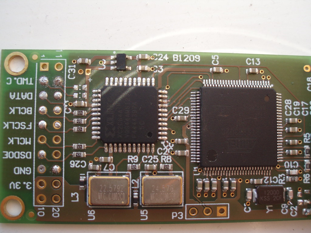
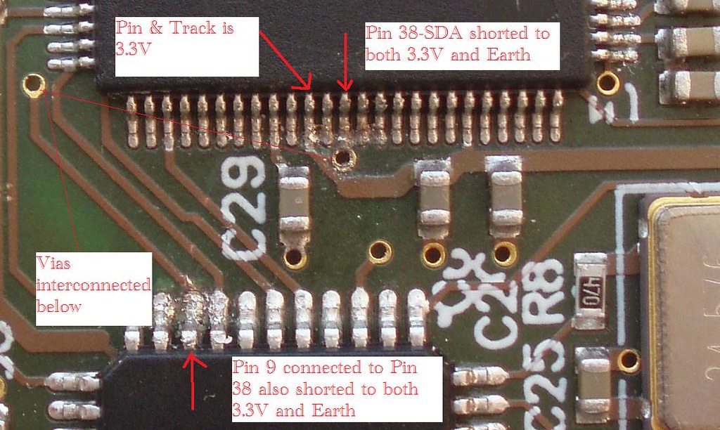
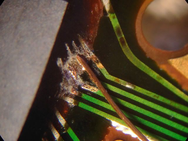
If you used VERY FINE enamelled wire, then the pins on the xFQP are not bent up much - note these pins break easily if bent too much... The Atmel chip is in a TQFP 100 package which has a pin pitch of only 0.5mm - pins & tracks on the PCB must be treated with respect.

With the removed chip, GENTLY press each edge in tun on a flat hard surface to align the pins and get them straight again. Clean the chip & pins with IPA - be very careful if using a cotton bud here as if a bit of cotton snags a pin, the pin can break...

So, now you have a clean chip and clean board. Using a flux pen, just wipe the pads gently with a tiny amount of flux (shouldn't need much - both pads & chip pins are already tinned)...

Align the chip ever so carefully over the pads making absolutely sure that pin 1 is in the right place - easy mistake to make with a square chip!

Tack a pin in one corner VERY CAREFULLY - re-tack until the chip seems well aligned on all 4 sides. Then tack a pin in the diametrically opposite corner. The chip should now be correctly lined up over the pads...

Using FINE (22AWG or similar) solder, preferably not with any extra flux in it (i.e. not Ersin muti-core etc.) just run the solder and the iron down each side in turn. Don't overload the pins or spend too long in any one area - also, don't worry about bridges between pins at this stage - we'll deal with that in a minute. The important thing here is that each pin is soldered to the pad beneath it, not how pretty the job is!

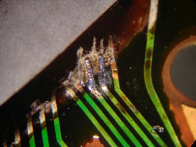
You now need a reel of fine solder wick - I use Chemtronics "Chem-Wik" with a size between 1 & 2mm, but any decent fine wick will do.

Lay the end of the wick along the whole of one side of the chip, over the newly soldered pins. Then starting at the end of the wick attached to the spool, press the soldering iron onto the top of the wick until you see some solder being absorbed (a few seconds) - slowly move the soldering iron down the row, gently lifting the wick off (whilst the solder in it is still molten so it doesn't stick to the pins) as its work is done. If the wick "sticks" to the pins - re-heat it gently - do NOT pull it as the pins may well break or a pad on the PCB may lift...

Miraculously (!!) as the wick lifts, you will be left with a perfectly soldered, clean, bridge & splash-free, row of pins. Repeat for the other sides. Note that if you really piled on the solder, you might need to repeat the wicking for a given side as fine wick doesn't absorb a huge amount of excess solder!!

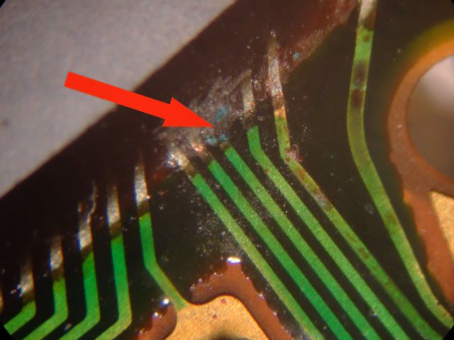
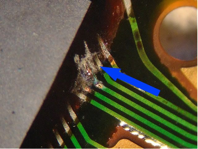
Inspect very carefully with USB 'scope, magnifying light etc. Clean with IPA & cotton buds. Inspect again !

The photo in my previous post shows how the pins look after wicking.

Note these two techniques work for pretty much any non-BGA, i.e. leaded, SMD device.

No disrespect to Amanero, but that board is ROUGH!

EDIT: Use IPA in a WELL VENTILATED AREA only - IPA fumes can (do) give you a blinding headache - really nasty - happened to me once - just like someone was smacking the front of my head HARD every few seconds with a shot-filled cosh... very unpleasant...

HTH
Last edited by jack on Mon Dec 17, 2012 9:56 pm, edited 2 times in total.
Vivitur ingenio, caetera mortis erunt
User avatar
Mike H
Amstrad Tower of Power
Posts: 20189
Joined: Sat Oct 04, 2008 5:38 pm
Location: The Fens
Contact:

#7

Post by Mike H »

Excellent tips. :D


How did you 'blow' the board? What were you doing?
 
"No matter how fast light travels it finds that the darkness has always got there first, and is waiting for it."
themystical
User
Posts: 65
Joined: Sun Aug 31, 2008 1:02 pm

#8

Post by themystical »

Nick wrote:It may not be that much help, but I am planning on using the same board for a dac I am working on. For that dac, the digital board I have designed is just about all surface mount. So to that end I have got myself a hot air rework station for about £90, not sure how good it is yet. And some illuminated magnifiers. So if no other options come about, you are welcome to come over to Halifax and try blowing hot air at it :-)
Nick
The board sounded excellent and I understand it can be improved further still by using low (lower?) noise supplies either via the USB at 5V or directly to the board at 3.3V having removed the on board regulator. Not tried these tweaks yet.
If it is okay with you, I might take you up on your offer, probably after Christmas, as 4 hands are probably better than 2 in this particular case and I can tap into your considerable expertise. :)
Avinash
themystical
User
Posts: 65
Joined: Sun Aug 31, 2008 1:02 pm

#9

Post by themystical »

spresto9 wrote:This helped me! good luck
http://www.youtube.com/watch?v=2ucIe4z532U
I took heart from that video. After all, my hands shake only marginally more than this guy's so I must be in with a chance. I have decided that I am definitely going for it so following nickds1's extraordinarily lucid advice, I have ordered:
This scalpel
http://www.ebay.co.uk/itm/281037498674? ... 1497.l2649
This dental tool kit
http://www.ebay.co.uk/itm/271098877087? ... 1497.l2649
and this USB Microscope
http://www.ebay.co.uk/itm/150781375030? ... 1497.l2649
The microscope is from HK so probably a two week wait but with Christmas in between, it shoudn't be too frustrating. :)
themystical
User
Posts: 65
Joined: Sun Aug 31, 2008 1:02 pm

#10

Post by themystical »

nickds1 wrote:Pretty much everything I do that's not valve-related has been SMD for years - its fun, but you do need decent kit & techniques.

Looking at that board, the soldering is pretty poor and there may well be bridges between pins - e.g. near C29. There also doesn't seem to be a solder mask or conformal coating on the board - this makes it extremely vulnerable to poor soldering and splashes/drops etc.

Desoldering the SMD xFQP devices can be done quite simply - using some fine enamelled wire and working on one side of each device at a time... the wire needs to be enamelled so that it doesn't stick to the pins you are desoldering...

HTH
Nick.....you are a true Master! Thanks for your articulate and lucid descriptions
How fine does the enamelled wire need to be? Is 0.1mm okay? I need to buy some.
I am amazed that you have commented about the poor soldering around C29.....the issues I am having relate to a pin in this area, see description of the fault in a seperate post below.
Avinash
themystical
User
Posts: 65
Joined: Sun Aug 31, 2008 1:02 pm

#11

Post by themystical »

Mike H wrote:Excellent tips. :D


How did you 'blow' the board? What were you doing?
it was all working fine in my "temporary" installation and then I decided to install it "permanently" in my DAC in a fairly complicated install which includes an Arduino with LCD Display and remote control including I2C connections from the Amanero Board. Something went wrong during this process and further investigation has revealed that Header Pin 12 (SDA) is now shorted to both the 3.3V bus and ground.
Well I am not completely sure but there were a couple of mishaps during the first switch on. I had got some of the wiring between the Arduino and LCD wrong and there were some shorts which both the Arduino and the LCD coped with. The Amanero board was also connected up at this point, no issues with the I2S connections to the DAC, but I also had the I2C (SDA Pin 12 and SCL Pin 2) connections from the Amanero board to the Arduino. As the Amanero board is not 5V tolerant on the I2C connections, I had the two lines powered via pull-up resistors from the 3.3V supplies on the Arduino and this is where I suspect the line might have ended up getting powered at 5V during the mishaps which may have "welded" the internal contact? Not completely sure.
Anyway I was intrigued by Nickds1's comments about the crap soldering around C29 so am posting the zoomed up piccy below explaining the issue to see if there are any comments.

Image
Marked Up Detail by themystical2012, on Flickr
Avinash
User avatar
jack
Thermionic Monk Status
Posts: 5502
Joined: Wed Dec 29, 2010 8:58 pm
Location: ɐılɐɹʇsnɐ oʇ ƃuıʌoɯ ƃuıɹǝpısuoɔ
Contact:

#12

Post by jack »

themystical wrote:Is 0.1mm okay? I need to buy some.
0.1mm is probably perfect - its fine enough to not move the pins too much, but strong enough not to break all the time... No finer than that, though, and do make sure its enamelled, not just tinned or plain copper...

The USB microscope you have mentioned on eBay is pretty much the same as the one I use - only point is that its depth of field is quite shallow, so keeping it in focus can be a pain - good devices though...

The Chemtronics Chem-Wik is also available on eBay (e.g. http://www.ebay.co.uk/itm/200795008502), as is a flux pen - I'd use a low-solids (no mess) flux pen like http://www.ebay.co.uk/itm/290829166314

The dental tools & scalpel blades look fine. The dental tools need to be stainless steel so they don't get "wetted" by molten solder...

A magnifying workbench light is a real asset for fine PCB work - search eBay for "magnifying light"...

The close-up seems to show a solder mask, so that's a bit of a help...

The board *may* just still be OK if you use some solder-wick to clean up those damaged areas - they do rather look like the aftermath of a short or two though (spatters of little blobs etc.) :( Is there something you're not telling us :)
Vivitur ingenio, caetera mortis erunt
Neal
Shed dweller
Posts: 2300
Joined: Fri Aug 03, 2007 10:57 am
Location: From the land of the Bodgers

#13

Post by Neal »

Reminds me of a PCB repair I had to make on a 70's digital watch. The battery has leaked an etched away many of the tracks. Most where reasonably easy to repair using a stereoscope and steady hand but the track to the main clock chip was a bar-steward.

Image

Image

I had to lay in the finest wire I could find and bridge the gaps.

Image

Image
simon
Thermionic Monk Status
Posts: 5643
Joined: Thu May 24, 2007 11:22 am
Location: People's Republic of South Yorkshire

#14

Post by simon »

themystical wrote:Well I am not completely sure but there were a couple of mishaps during the first switch on.
You're in good company here!
simon
Thermionic Monk Status
Posts: 5643
Joined: Thu May 24, 2007 11:22 am
Location: People's Republic of South Yorkshire

#15

Post by simon »

Neal wrote:Reminds me of a PCB repair I had to make on a 70's digital watch.
Blimey Neal, fair play to you. Must have been some watch to go to all that trouble for?
Post Reply